Search Microcontrollers

Showing posts with label Stellaris. Show all posts

Monday, April 6, 2015

Stellaris Launchpad - NRF24L01 radio - Part 2

Ok, I had this one in draft for long enough now.
I still need to figure out a few things, so a part 3 will be needed in the future, also I initially had issues with Dynamic Payloads as I forgot to issue the FEATURE = EN_DPL command, hopefully shoudl work better now.


In a previous post we saw some basic concepts and functionality of the NRF24L01 chip.

We managed to establish a SPI communication between the Stellaris and the module, but we did not perform any data transmission across two nodes.
to achieve that we need to add a few functions to our library and decide some basic defaults for it.

I think this automatic ACK system (if you don't know what I am talking about, you really need to read my previous post) is pretty cool and I think it would be fair to use it by default, so the library will assume we are going to use it, should we have any issues with it later on, we might eventually change approach.

While supporting multiple RX pipes is indeed interesting, so I would rather keep that functionality in the library, we can assume that, by default, communication will be through pipe0.

The function nrf_enablePipes accepts a byte (bits 0:5 represent the 6 pipes) does 3 things :

1) Enables the selected pipes
2) Activates the AUTO ACK magic for them
3) configures them for dynamic payload

void nrf_enablePipes(unsigned char pipes)
{
  nrf_writeReg(EN_AA, pipes);     
         // enable AUTO ACK on pipes
  nrf_writeReg(EN_RXADDR, pipes); // enable pipes
  nrf_writeReg( FEATURE, 1<<EN_DPL ); //enable DPL
  nrf_writeReg(DYNPD, pipes); // dynamic payload for pipes
}

About dynamic payload (DPL), the Datasheet says :

(@Nordic)


Another default I picked is to use 5 byte addressing.

Now we need to be able to set the TX address and the various RX addresses for the RX pipes.

 /*
#define RX_ADDR_P0  0x0A
#define RX_ADDR_P1  0x0B
#define RX_ADDR_P2  0x0C
#define RX_ADDR_P3  0x0D
#define RX_ADDR_P4  0x0E
#define RX_ADDR_P5  0x0F
pipe : 0..5
 */
void nrf_setRXAddress(unsigned char pipe, unsigned char *addr)
{
 nrf_writeRegMulti(RX_ADDR_P0+pipe, addr, 5);
}

void nrf_setTXAddress(unsigned char *addr)
{
 nrf_writeRegMulti(TX_ADDR, addr, 5);
}

the writeRegMulti function works like the writeReg, but accepts a buffer and sends n bytes instead of a single one, we need it for setting the addresses since they are 5 bytes long.

As we discussed in the previous post, a node can be set up as PRX or PTX, this is done setting the lowest bit in the CONFIG register : 1 means PRX, 0 means PTX.
The same register is used to specifcy if a CRC is used, int hat case wether is it 1 or 2 byte long,m plus there are 3 bits used to mask the interrupts.

You can find more info on the CONFIG register here.

/**
 * Set crc = 0 to disable crc, 1 for 1 byte ,2 for 2 bytes
 */
void nrf_config(unsigned char maskRXirq, 
                unsigned char maskTXirq,
                unsigned char maskMAXirq,
unsigned char crc,
                unsigned char pwUp,
                unsigned char prx)
{
   unsigned char val = maskRXirq<<6 | 
                       maskTXirq<<5 | 
                       maskMAXirq <<4;
   if (crc>0) val |= 8; else crc--;
   val |= crc <<2 | pwUp<<1 | prx;
   nrf_writeReg(CONFIG,val);
}

When we need to initiate a transmission, we need to set up the node as PTX, to set the TX address to the address of the receiving module, plus the Pipe0 address equal to the TX one.

Additionally we might want to configure the number of transmission attempts (if Auto ACK fails) and the delay between them

/**
 * delay : 0 = 250us, 1=500us ... 15=4000us
 * count : 0..15 auto retransmit if AA fails
 */
void nrf_setRetransmit(unsigned char count, 
                       unsigned char rDelay)
{
 unsigned char val = ((rDelay&0x0f)<<4) | (count&0x0f);
 nrf_writeReg(SETUP_RETR,val);
}

In our experiment we will use node 1 with address "node1" (in ASCII) and node 2 with address "node2" and we will try to have them communicate  @2MBps on the channel 0x10.
Node 1 will try to send a payload containing the data "TEST1234" every 2 seconds and we will use the RGB leds on the two Launchpads to provide some feedback.

For this initial test we will do something simple, however I believe we still need to use two pipes.
The reason for this is that when the PTX sends data, it has to configure the RX pipe0 with the same address of the receiver, therefore it needs to be able to listen on a different pipe, with a unique address, in order to be contacted when it switches back to PRX.

Initially I was thinking to have one of the two nodes running on Arduino, to use a know library such as Mirf to minimize the debug, unfortunately I am not really sure if Mirf allows to be configured properly and if that is the case, I don't know how, while with my library at least I know all the settings.

Ok, I stopped here because I got lost with the DPL feature, as stated at the beginning, should work now, need to experiment a bit more (been doing other stuff for quite some time) and then hopefully a final Part 3 will be posted :) 

Saturday, April 26, 2014

Stellaris Launchpad - NRF24L01 radio - Part 1

I have a couple of digital radio transceivers hanging around my desk since quite some time, so I decided to finally try them out.

These are cheap Nortel NRF24L01 devices, it is common to find them in small breakout modules that communicate via SPI protocol.


Some have an 8 pin connection, some others a 10 pins one, they are just the same in fact since the 10 pins one have 2 VCC and 2 GND pins, normally pins are marked on the silkscreen.

WARNING : The chip works at 3.3V (VCC) which is fine with the Stellaris, but should you use it with an arduino or another 5V MCU make sure you provide a proper VCC. The digital signals are also at 3.3V, but they are 5V tolerant.

There are popular libraries for Arduino / AVR for them and even a Stellaris library for the Energia environment  ( Arduino-like for the Stellaris Launchpad).

I actually prefer to use them in my common environment, plain CCSV5 with driverlib support, so I decided to write my own module.

You can find the datasheet of the module here (Sparkfun site, they sell those little boards too).

I reverse engineered code snippets found on the web, from the various libraries and managed to write my own code.

First off, since we are dealing with a SPI connection we are going to have  a SCLK, MISO , MOSI connection, plus a CE (Chip Enable), a CSN and an IRQ generated by the module itself.
So, it is a sort of " rich" SPI interface.
While the first three (MISO, MOSI and  SCLK) are managed directly by the SSI module of the Cortex M4F, we still need to manage manually the other three signals using 3 GPIO conections, two outputs and 1 input for the IRQ.

I decided to use SPI on port SSI1 (uses pins D.0, D.2, D.3) and the GPIO port E to drive CE, CSN and IRQ -E.1, E.2, E.3- (I saw a library on the web using this setup and found it quite smart, since the connections are all aligned on the launchpad connector).
I stored these values in variables, just to allow for some flexibility in configuration

unsigned long NRF_GPIO = GPIO_PORTE_BASE;
unsigned long NRF_PERIPH_GPIO = SYSCTL_PERIPH_GPIOE;
unsigned char CEPIN    = GPIO_PIN_1;
unsigned char CSNPIN   = GPIO_PIN_2;
unsigned char IRQPIN   = GPIO_PIN_3;

Then I created an init function to enable the needed ports, set up the SPI etc :

void setSPI()
{
  unsigned long dummy = 0;
  SysCtlPeripheralEnable(SYSCTL_PERIPH_SSI1);
  SysCtlPeripheralEnable(SYSCTL_PERIPH_GPIOD); // SPI
  SysCtlPeripheralEnable(NRF_PERIPH_GPIO); // CS, CE, IRQ
  GPIOPinConfigure(GPIO_PD0_SSI1CLK);
  GPIOPinConfigure(GPIO_PD1_SSI1FSS);
  GPIOPinConfigure(GPIO_PD2_SSI1RX);
  GPIOPinConfigure(GPIO_PD3_SSI1TX);
  GPIOPinTypeSSI(GPIO_PORTD_BASE, GPIO_PIN_3 | GPIO_PIN_2 | GPIO_PIN_1 | GPIO_PIN_0);
  SSIConfigSetExpClk(SSI1_BASE, SysCtlClockGet(),
                 SSI_FRF_MOTO_MODE_0,
         SSI_MODE_MASTER, 1000000, 8);
  SSIEnable(SSI1_BASE);
  GPIOPinTypeGPIOOutput(NRF_GPIO, CEPIN| CSNPIN);
  GPIOPinTypeGPIOInput(NRF_GPIO, IRQPIN);
  while(SSIDataGetNonBlocking(SSI1_BASE, &dummy))
   {}
}

The while cycle at the end is there just to remove from the FIFO whatever garbage data might be eventually present.

The NRF24L01 chip is quite versatile, can operate on various channels and can easily manage communication on a network of addressable devices.
To allow this flexibility, the chip is configured with a set of registers, so the first thing we need to implement are the functions to read from and write to these registers, plus the CE / CSN handling.

The process is quite simple :
Each register has a 5 bit address (documented in the data sheet, but since I am lazy I just imported an existing .h file that defined them all -you can find it here-) and if we combine these 5 bits (r rrrr) with 001 in the 3 MSBs (001r rrrr) then we have a 1 byte command that, when delivered via SPI, tells the chip we want to write the register r rrrr.
The following byte is the value we want to store in the specified register.
Reading is similar , but we will add 000 in the 3 MSBs instead, so the command for reading r rrrr is 000r rrrr .
Details about reading values will be discussed later.

However, for the chip to respond we need to properly manage the CE and CSN signals.

The chip is enabled when CE is asserted LOW and when there is no communication from the master, CSN should be HIGH, so this is our initial setting.
Then, before sending data via SPI, CSN must be transitioned to LOW and finally back HIGH once the communication (writes + reads) is terminated.

void setCE(unsigned char val)
{
  if (val>0)
 GPIOPinWrite(NRF_GPIO, CEPIN ,CEPIN); //CE HIGH
  else
GPIOPinWrite(NRF_GPIO, CEPIN ,0); //CE LOW
}

void setCSN(unsigned char val)
{
  if (val>0)
GPIOPinWrite(NRF_GPIO, CSNPIN ,CSNPIN); //CSN HIGH
 else
  GPIOPinWrite(NRF_GPIO, CSNPIN,0); //CSN LOW
}

The two setCxx functions are quite obvious, not particularly elegant I have to admit, but they get the job done.

void sendChar(unsigned char ch)
{
  SSIDataPut(SSI1_BASE, ch);
  while(SSIBusy(SSI1_BASE)) {}
}

sendChar is a helper function that outputs a byte to the SPI port, I added a while loop to ensure data is flushed out before leaving the function, I am not 100% sure we need that, but it helped me when debugging the line with my DSO.

void _writeReg(unsigned char addr, unsigned char val)
{
  setCSN(0);
  sendChar(W_REGISTER | addr);
  sendChar(val);
  setCSN(1);
}

unsigned long _readReg(unsigned char addr)
{
  unsigned long result = 0xff;
  setCSN(0);
  sendChar(R_REGISTER | addr);
  while(SSIDataGetNonBlocking(SSI1_BASE, &result)){}
  sendChar(0xf0); //whatever value, used 0xf0 because 
      // it is easily visible with the oscilloscope
  SSIDataGet(SSI1_BASE, &result);
  setCSN(1);
  return result;
}

_writeReg is quite a straightforward implementation of what I described before (W_REGISTER = 0010 0000) while _readReg is a bit trickier :
First thing notice the while loop used to throw away data right after the read register command.
This is needed (you can check it with an oscilloscope on the RX (MISO) line of the MCU) because as soon as you start sending data on the TX channel (MOSI), the slave device writes garbage data on the RX (typically a 0x0E value I found in my experiments).

After you sent the command, then, you need to send out a dummy byte (it does not matter the value) per each byte you need to read -in this case 1- and finally read the value and bring CSN high.


[You can see in yellow the MOSI line, roughly between the two purple vertical cursors there is the first byte. In red the MISO line is immediately answering with "garbage" data which I suspect is in fact the status of the module.
It is easy to recognize the second dummy byte being 0xF0 and then we get a (correct) response 0x03 on the MISO]

I then found a sequence of "default" values of the registers used to init the module :

void nrfInit()
{
  unsigned long dummy =0;
  _writeReg(CONFIG, 0x00);  // Deep power-down, everything disabled
  _writeReg(EN_AA, 0x03);
  _writeReg(EN_RXADDR, 0x03);
  _writeReg(RF_SETUP, 0x00);
  _writeReg(STATUS, ENRF24_IRQ_MASK);  // Clear all IRQs
  _writeReg(DYNPD, 0x03);
  _writeReg(FEATURE, EN_DPL);  // Dynamic payloads enabled by default
  SysCtlDelay(SysCtlClockGet() / 100 / 3); // grace time, never hurts 
  while(SSIDataGetNonBlocking(SSI1_BASE, &dummy)) {}
}

So, the init overall sequence is :
setSPI();
setCE(0);
setCSN(1);
nrfInit();

I also found that a way to check if the connection with the module is working is to check the value of the SETUP_AW register, which should return 6 MSBs = 0 and the two LSB with 01 (3byte address) ,10 (4 bytes) or 11 (5 bytes) while 00 means illegal number.


int _isAlive()
{
  unsigned long aw;
  aw = _readReg(SETUP_AW);
  return ((aw & 0xFC) == 0x00 && (aw & 0x03) != 0x00);
}

At this point, we can check if the basic communication via SPI works :

#include <inc/hw_memmap.h>
#include <inc/hw_types.h>
#include <driverlib/gpio.h>
#include <driverlib/sysctl.h>
#include <driverlib/uart.h>
#include <inc/hw_timer.h>
#include <driverlib/timer.h>
#include <driverlib/pin_map.h>
#include <utils/uartstdio.c>
#include "driverlib/ssi.h"
#include "nRF24L01.h"

void setClock()
{
   SysCtlClockSet(  SYSCTL_SYSDIV_4 | SYSCTL_USE_PLL |
        SYSCTL_XTAL_16MHZ  | SYSCTL_OSC_MAIN);
}

....

int main(void) {
 setClock();
 // we  use the led to provide feedback
  SysCtlPeripheralEnable(SYSCTL_PERIPH_GPIOF);
  GPIOPinTypeGPIOOutput(GPIO_PORTF_BASE, GPIO_PIN_2 | GPIO_PIN_1 | GPIO_PIN_3);
  GPIOPinWrite(GPIO_PORTF_BASE, GPIO_PIN_2 | GPIO_PIN_1 | GPIO_PIN_3, 0); // LED OFF

 setSPI();
 enableNRF();
 SysCtlDelay(SysCtlClockGet() / 10 / 3);
 nrfInit();
 if (_isAlive()!=0)
  GPIOPinWrite(GPIO_PORTF_BASE, GPIO_PIN_3, GPIO_PIN_3); // GREEN
 else
  GPIOPinWrite(GPIO_PORTF_BASE, GPIO_PIN_3, 0); // OFF
} // main

Ok, so far we implemented the basic communication with the module, now we need to investigate how the radio data transmission happens.

Reading the Nortel datasheet shows some complexity and also allows us to understand that these devices can be operated in quite a few different ways.

Some basic concepts : 
In a network, at a given time, we identify one PTX and one  PRX, these stand for Primary Transmitter and Primary Receiver.
Obviously we are dealing with a Transceiver, so this module can send and receive data.

Table 12 in the Datasheet shows the different states we can set the module


(@Nordic)

For the actual data transmission, a mechanism called "Enhanced ShockBurst"(TM) is used, Nordic defines it as "a packet based data link layer".

What this layer does is to take care of the delivery of payloads (strings of data with 0 to 32 bytes content) from a TX to an RX station.

Enhanced ShockBurst has an automatic handling which automated a few basic actions for us, as an example, after a PTX finished sending out a packed of data, it cnverts it automatically to PRX to be ready to receive an ACK packet.
ACK packets can be also generated automatically if the module is configured to do so.
In fact in the init procedure we have a  _writeReg(EN_AA, 0x03); instruction which enable this Auto ACK feature.
If an ack is not received, then the PTX will retry to send the packet a number  of times, automatically.
To prevent that a packet is read twice (duplicating the data) a PID (Packet Identification) is associated to each packet, a CRC is also used to verify if data is correct.

The packet itself is composed by different sections (Preamble, Address, packet control field, payload and CRC), but it is properly assembled by the device itself using an automatic packet assembly functionality.

Similarly a packet is decoded (disassembled) automatically on the RX side.

An important feature,m on the RX side, is the Multiceiver.
In fact each receiver can use up to 6 data pipes, each one responding on a different address.
There is no magic here, one single channel is used at a time, so you cannot stream different payloads to different pipes at the same time, this functionality is there mainly to allow you to logically separate data streams, for whatever need you might have.

Addresses can be 3, 4 or 5 bytes (can be configured via the SETUP_AW register), so, assuming we are using 5 byte addresses some rules apply: 

1) the lower by is unique across all the pipes
2)  pipes 1 to 5 have the same 4 high bytes

When using the multiceiver feature, the PRX can receive packets from multiple PTXs (on different pipes), it stores on each pipe the "return address" of the TX and uses it to send automated ACK packets.

Specific registers RX_ADDR_Px are used to specify the RX addresses for the 6 pipes, each of these registers is 5 byte wide.

An example of multiceiver configuration (from the nrf24l01 datasheet) is reported here


(@Nordic)

So, our next step will be to write the functions that set up the channel, the TX and RX Addresses and finally that deliver a payload.
While I work on that, you might as well go through the datasheet.

[to be continued]

Friday, April 11, 2014

Stellaris Launchpad - Stepper Motors

I just noticed I had a post in my drafts, almost ready to be published, it was lying there since some time...

Stepper motors are fun, right?
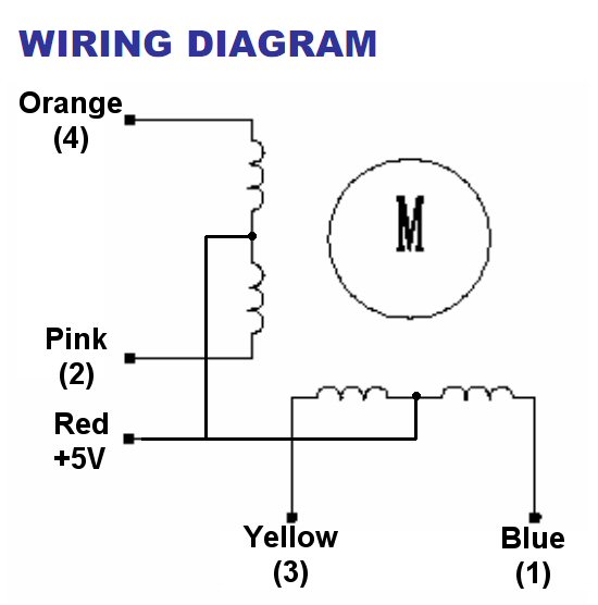
You can easily find cheap stepper motors that can be driven by MCUs, they need a driver circuit as MCUs cannot provide enough current via their GPIO ports, but these drivers are normally just a set of simple transistors.

I experimented with a  small 28BYJ 5V Stepper Motor which contains a gearbox that allows it to deliver a decent torque and precision (sacrificing the rotation speed).


There are libraries for Arduino and maybe even for ARM Cortex MCUs, not sure about that, but, as usual, I wanted to get my fingers dirty and experiment a bit.

A typical driver for this motor is the ULN2003 driver, which is just a darlington array that delivers just enough juice for the 28BYJ (500mA).
Those darlingtons can also be activated via a 3.3V GPIO, base resistors and protection diodes are already included in the package... pretty easy, no?


For the 28BYJ only 4 transistors are used, common is connected to +5V.
You need an external power supply to provide this 5V as you need 500mA, remember to connect the ground of the additional PSU to the launchpad ground.

So, the circuit itself is quite simple, I used a simple board for the ULN2003, which I bought together with the motor (it is quite common) so I did not have to mess around with soldering etc.


The motor has 4 phases that must be activated in the correct sequence of 8 steps to obtain a clockwise rotation or in the opposite sequence should you want to achieve a counter-clockwise one.

Easiest thing to do is to create an array with the 4 bits and the 8 steps cycle.

unsigned char steps[8] ={0b0001,0b0011,0b0010,0b0110,0b0100,0b1100,0b1000,0b1001};

each one of those bits should be addressed to a GPIO pin, I used pins  D.0, D.1, D.2 and D.3 which can be found on the J3 connector of the launchpad. 

So, the first step 0b0001 would set D.0 high and the three other ones low.

I then decided to use a timer with an associated interrupt to cycle the steps.
Setting the timer value is key because we are dealing with a  mechanical thing here, it has inertia and therefore can reach a maximum rotation speed that cannot be exceed (it would stall).
Setting the correct speed depends also on the load you have attached to the motor.

Of course providing a nice acceleration ramp lets you achieve higher rotation speeds, however I am not sure it is a good idea in a real application because if the motor misses a few steps due to exceptional load, then you might be driving it at a speed it cannot achieve starting from zero, and would remain stalled. 
You can try that, simply block the rotation when it runs faster than it can from still and see what happens.


Ok, back to my test program.
I wanted to use the two user switches on the launchpad to make it rotate 180deg in each direction.

I then created a variable int cntSteps = 0;  which represents the number of steps to be executed, if it has  a negative value then I will traverse the steps array backwards.
This is done in the nextStep() procedure.
I also need a int step variable to identify the position within the array of the current step.

void nextStep()
{
if (cntSteps>0)
{
GPIOPinWrite(GPIO_PORTF_BASE, GPIO_PIN_1|GPIO_PIN_2|GPIO_PIN_3,GPIO_PIN_1); //red
if (step<7) step++; else step=0;
    cntSteps--;
}
else
{
GPIOPinWrite(GPIO_PORTF_BASE, GPIO_PIN_1|GPIO_PIN_2|GPIO_PIN_3,GPIO_PIN_2); //blue
if (step>0) step--; else step=8;
cntSteps++;
}
GPIOPinWrite(GPIO_PORTD_BASE, 0x0f, steps[step]&0x0f);
}

Depending on the sign of the cntSteps variable I cycle through the array and finally output the 4 bit value (masked, just in case) to the GPIO port D.
I also added a blue led on if turning in one direction and red if turning in the opposite one.
When the motor is still, the LED is green indicating the system is ready to receive another command. 

This is visible in the Time Interrupt Handler (you can find more info on interrupts here)

// timer interrupt handler
void timerIntHandler(void)
{
   TimerIntClear(TIMER0_BASE, TIMER_TIMA_TIMEOUT);
    if (cntSteps!=0)
    nextStep();
    else GPIOPinWrite(GPIO_PORTF_BASE, GPIO_PIN_1|GPIO_PIN_2|GPIO_PIN_3,GPIO_PIN_3);
}

If we need to move (cntSteps!=0) then the next  Step is executed else, the LED is turned green.

Interrupt handlers must be registered, that's  done in the setup_ccs.c file of the project, in the #pragma DATA_SECTION(g_pfnVectors, ".intvecs") structure.


In my case, I used two interrupt handlers, one for the two switches and one for the timer0_A, I located the position of the GPIO PORT F and TIMER 0 A and then replaced the defaultHandler with the procedures I created in my main.c file.

Since these procedures are defined in main.c, you need to declare the external before the int vec structure we just discussed, still in startup_ccs.c :

//------------- custom int handlers
extern void timerIntHandler(void);
extern void switchIntHandler(void);

Ok, now let's see how the user switch interrupt handler works.

// switch interrupt handler
void switchIntHandler(void)
{
GPIOPinIntClear(GPIO_PORTF_BASE,GPIO_PIN_0
                                       |GPIO_PIN_4);
if (cntSteps==0)
{
if (GPIOPinRead(GPIO_PORTF_BASE,
                          GPIO_PIN_0|GPIO_PIN_4)
                        &GPIO_PIN_4 > 0)
                 addAngle((double)180.0f);
else addAngle((double)-180.0f);
}

}

As you can see I created a single handler for both switches, this is possible because they are both on the same GPIO port (F).
Using the interrupt on F.0 is not trivial and requires some funny coding, but I will dig into that later.

The addAngle procedure is quite simple, it converts an angle into a number of steps knowing that there are a total of 4076 steps in 360 degrees (not really sure of that value, I found it online, you may want to double check eventually) taking into account also the reduction gears.

// -- adds a specific number of steps depending on the needed angle
void addAngle(double deg) // 4076 steps
{
double newAngle =deg*4076/360;
  cntSteps += newAngle;
}

Finally , we are just missing the setup part.

// configure mcu clock speed
void setClock()
{
 //25 MHZ
 SysCtlClockSet(  
         SYSCTL_SYSDIV_8 |SYSCTL_USE_PLL 
         SYSCTL_XTAL_16MHZ  | SYSCTL_OSC_MAIN);
}

// stepper timer setup
void setTimer(int stepsPerSec)
{
    SysCtlPeripheralEnable(SYSCTL_PERIPH_TIMER0);
    TimerConfigure(TIMER0_BASE, TIMER_CFG_PERIODIC);
    TimerLoadSet(TIMER0_BASE, TIMER_A, 
            SysCtlClockGet()/ stepsPerSec);
    IntEnable(INT_TIMER0A);
    TimerIntEnable(TIMER0_BASE, TIMER_TIMA_TIMEOUT);
    TimerEnable(TIMER0_BASE, TIMER_A);
}

These two procedures set up the MCU clock to 25MHz and prepare the timer to fire an interrupt stepsPerSec times each second.
We are just missing the gpio setup part and here I had to do something  a bit unconventional.
If you check the launchpad schematics, you will notice that the user switch 2 has an additional connection called WAKE


Practically by default this switch generates an NMI (Non Maskable Interrupt) used to wake the CPU from sleep modes.
Unfortunately this functionality interferes with the Interrupt handler for SW2 (D.0), unless you " massage"  it properly.

  //workaround for pin_0 to nmi
    HWREG(GPIO_PORTF_BASE + GPIO_O_LOCK) =   GPIO_LOCK_KEY_DD;
    HWREG(GPIO_PORTF_BASE + GPIO_O_CR) |= 0x01;
    HWREG(GPIO_PORTF_BASE + GPIO_O_LOCK) = 0;
I am note really sure what it does, I just found it online and it works, you add that to your GPIO configuration and magically sw2 can be serviced with an interrupt handler.

The complete GPIO setup is as follows :

// GPIO & Interrupt configuration
void setGPIO()
{
SysCtlPeripheralEnable(SYSCTL_PERIPH_GPIOF); 
  // to read switches
SysCtlPeripheralEnable(SYSCTL_PERIPH_GPIOD); 
  // used to output stepper signals

GPIOPadConfigSet(GPIO_PORTD_BASE, // identifies the GPIO PORT
0x0f,                 // identifies the pin within the GPIO Port
GPIO_STRENGTH_8MA_SC, // sets the strength to 8mA with Slew Rate control
GPIO_PIN_TYPE_STD);   // sets the pad control type to push-pull
GPIOPinTypeGPIOOutput(GPIO_PORTD_BASE, GPIO_PIN_0|GPIO_PIN_1|GPIO_PIN_2|GPIO_PIN_3);

    // setup LEDs
GPIOPinTypeGPIOOutput(GPIO_PORTF_BASE, GPIO_PIN_1|GPIO_PIN_2|GPIO_PIN_3);
GPIOPadConfigSet(GPIO_PORTF_BASE,
GPIO_PIN_1|GPIO_PIN_2|GPIO_PIN_3,
GPIO_STRENGTH_8MA_SC,
GPIO_PIN_TYPE_STD);
    //turn LEDs off
GPIOPinWrite(GPIO_PORTF_BASE, GPIO_PIN_1|GPIO_PIN_2|GPIO_PIN_3,0);

    IntMasterEnable(); // enable processor interrupts

    //workaround for pin_0 to nmi
    HWREG(GPIO_PORTF_BASE + GPIO_O_LOCK) = GPIO_LOCK_KEY_DD;
    HWREG(GPIO_PORTF_BASE + GPIO_O_CR) |= 0x01;
    HWREG(GPIO_PORTF_BASE + GPIO_O_LOCK) = 0;

    // set the two switches as inputs
GPIOPinTypeGPIOInput(GPIO_PORTF_BASE,GPIO_PIN_0|GPIO_PIN_4);
GPIOPadConfigSet(GPIO_PORTF_BASE, GPIO_PIN_0|GPIO_PIN_4,
         GPIO_STRENGTH_4MA,
         GPIO_PIN_TYPE_STD_WPU); // configure input pads
// interrupt set to falling edge since the switches are normally "high"
// they indeed know how to have fun, lol :P
GPIOIntTypeSet(GPIO_PORTF_BASE,GPIO_PIN_0|GPIO_PIN_4, GPIO_FALLING_EDGE);
GPIOPortIntRegister(GPIO_PORTF_BASE,switchIntHandler);
GPIOPinIntEnable(GPIO_PORTF_BASE,GPIO_PIN_4|GPIO_PIN_0);
}

If you check again the switch schematics, you will notice that when they are pressed, they are connected to ground, so it is appropriate to use a falling_edge interrupt to detect when they are pressed.
In my case this is important because I am using a single ISR for both switches and I need to check which one is pressed, if I used a raising_edge interrupt, the ISR would have been activated when the button was released and I could not tell which one of the two was released by reading the GPIO port.

finally, the main cycle is trivial :

int main(void) {
 setClock();
 setGPIO();
 cntSteps = 0;
 setTimer(800);//steps per second
 while (1) {}// do nothing, interrupts will handle that
} // main
You can find the full code here

Have fun with stepper motors, interrupts and switches!
Should you be looking for this stepper motors, chances are you can find it cheap here :

Sunday, March 2, 2014

Stellaris Launchpad - PWM Library

I played a bit with PWM, which I actually need to drive a laser diode (2.4W 808nm) at the moment (will dig into this probably more in future posts).
Once you get the basics PWM is not difficult with the LM4F, however I found way easier for my application to create a minimalist library to deal with PWM signals, each time I look at it I keep repeating to myself that it could be better... but the way it is now already fits my needs (and maybe yours, but feel free to improve it and let me know :) ).

One thing I wanted was to have a simple interface that would allow me to play with multiple PWM generators at the same time, 8 seemed a fair amount, so I pre-allocated an array of 8, but it is fairly easy to expand the array.
Meh, some range checking would help maybe, but the Stellaris does not run on MS Windows, so it does pretty much what you tell it to do, just be careful not to add more than 8 pwm or at least remember to expand the array and you should be fine.

That said, each pwm generator is actually coming from a timer, we can use 16 bit or 32 bit timers and I figured that a 16 bit timer would do (did not try yet, but I think I found how to use it in 32 bit mode).
Still I did not implement pre-scaling which could be beneficial if you have to run with very low frequencies (<2Hz).

Here's  the library (don' t expect anything fancy, it's  just easy to use and actually works)


#include <inc/hw_memmap.h>
#include <inc/hw_types.h>
#include <driverlib/gpio.h>
#include <driverlib/sysctl.h>
#include <driverlib/uart.h>
#include <inc/hw_timer.h>
#include <driverlib/timer.h>
#include <driverlib/pin_map.h>

int pwm_count = 0;
int pwmtimers[8][4];

/**
 * each timer can send the signal out to 2 different gpios
 * 0 means to set it to the lowest of the two 1 to the highest
 *
 * TIMER    PIN(gpio=0) PIN(1)
 * T0A         PB6 PF0
 * T0B PB7 PF1
 * T1A PB4     PF2
 * T1B          PB5     PF3
 * T2A          PB0     PF4
 * T2B          PB1     PB1
 * T3A          PB2     PB2
 * T3B          PB3     PB3
 *
 *
 *
 */
int addPWM(int pwm_timer,int subtimer, int gpio) {
pwmtimers[pwm_count][0] = pwm_timer;
pwmtimers[pwm_count][1] = subtimer;
if (gpio == 0) {
if ((int)subtimer == (int)TIMER_A) {
switch (pwm_timer) {
case TIMER0_BASE:
pwmtimers[pwm_count][2] = GPIO_PIN_6;
pwmtimers[pwm_count][3] = GPIO_PB6_T0CCP0;
break;
case TIMER1_BASE:
pwmtimers[pwm_count][2] = GPIO_PIN_4;
pwmtimers[pwm_count][3] = GPIO_PB4_T1CCP0;
break;
case TIMER2_BASE:
pwmtimers[pwm_count][2] = GPIO_PIN_0;
pwmtimers[pwm_count][3] = GPIO_PB0_T2CCP0;
break;
case TIMER3_BASE:
pwmtimers[pwm_count][2] = GPIO_PIN_2;
pwmtimers[pwm_count][3] = GPIO_PB2_T3CCP0;
break;
}
} else {
switch (pwm_timer) {
case TIMER0_BASE:
pwmtimers[pwm_count][2] = GPIO_PIN_7;
pwmtimers[pwm_count][3] = GPIO_PB7_T0CCP1;
break;
case TIMER1_BASE:
pwmtimers[pwm_count][2] = GPIO_PIN_5;
pwmtimers[pwm_count][3] = GPIO_PB5_T1CCP1;
break;
case TIMER2_BASE:
pwmtimers[pwm_count][2] = GPIO_PIN_1;
pwmtimers[pwm_count][3] = GPIO_PB1_T2CCP1;
break;
case TIMER3_BASE:
pwmtimers[pwm_count][2] = GPIO_PIN_3;
pwmtimers[pwm_count][3] = GPIO_PB3_T3CCP1;
break;
}
}
} else if (subtimer == TIMER_A) {
switch (pwm_timer) {
case TIMER0_BASE:
pwmtimers[pwm_count][2] = GPIO_PIN_0 | 0x100; // port F
pwmtimers[pwm_count][3] = GPIO_PF0_T0CCP0;
break;
case TIMER1_BASE:
pwmtimers[pwm_count][2] = GPIO_PIN_2 | 0x100;
pwmtimers[pwm_count][3] = GPIO_PF2_T1CCP0;
break;
case TIMER2_BASE:
pwmtimers[pwm_count][2] = GPIO_PIN_4 | 0x100;
pwmtimers[pwm_count][3] = GPIO_PF4_T2CCP0;
break;
case TIMER3_BASE:
pwmtimers[pwm_count][2] = GPIO_PIN_2;
pwmtimers[pwm_count][3] = GPIO_PB2_T3CCP0;
break;
}
} else { // timer B
switch (pwm_timer) {
case TIMER0_BASE:
pwmtimers[pwm_count][2] = GPIO_PIN_1 | 0x100;
pwmtimers[pwm_count][3] = GPIO_PF1_T0CCP1;
break;
case TIMER1_BASE:
pwmtimers[pwm_count][2] = GPIO_PIN_3 | 0x100;
pwmtimers[pwm_count][3] = GPIO_PF3_T1CCP1;
break;
case TIMER2_BASE:
pwmtimers[pwm_count][2] = GPIO_PIN_1;
pwmtimers[pwm_count][3] = GPIO_PB1_T2CCP1;
break;
case TIMER3_BASE:
pwmtimers[pwm_count][2] = GPIO_PIN_3;
pwmtimers[pwm_count][3] = GPIO_PB3_T3CCP1;
break;
}
}
return pwm_count++;
}

/**
 *
 */
void pwmStop(int pidx) {
TimerDisable(pwmtimers[pidx][0], pwmtimers[pidx][1]);       
 //enables timerx_y
}

/**
 *
 */
void pwmStart(int pidx) {
TimerEnable(pwmtimers[pidx][0], pwmtimers[pidx][1]);        
//enables timerx_y
}

/**
 * Frequency in HZ and Duty cycle in %
 * example : pwm_setFreqDC(0,25000,0.3)  sets 25KHz with 30% duty cycle
 */
void pwmSetFreqDC(int idx, int freq,double dutyCycle) {
int period = (SysCtlClockGet() / freq);
int pidx = idx;
TimerLoadSet(pwmtimers[pidx][0], 
                     pwmtimers[pidx][1], period - 1); // sets pwm period
TimerMatchSet(pwmtimers[pidx][0], 
                     pwmtimers[pidx][1], period *dutyCycle); // sets duty cycle
}


/**
 *
 */
void pwmConfigure(int idx) {
int timerp = 0;
// ENABLE gpio port
int gpioPort;
volatile int pidx = idx;

if ((pwmtimers[pidx][2] & 0x100) > 0) { // pidx changes value here ????

SysCtlPeripheralEnable(SYSCTL_PERIPH_GPIOF);
gpioPort = GPIO_PORTF_BASE;
} else {

SysCtlPeripheralEnable(SYSCTL_PERIPH_GPIOB);
gpioPort = GPIO_PORTB_BASE;
}

// configure gpio pin
GPIOPinTypeGPIOOutput(gpioPort, pwmtimers[pidx][2] & 0xff);
GPIOPadConfigSet(gpioPort, // identifies the GPIO PORT
pwmtimers[pidx][2] & 0xff,  // identifies the pin within the GPIO Port
GPIO_STRENGTH_8MA_SC, // sets the strength to 8mA with Slew Rate control
GPIO_PIN_TYPE_STD);   // sets the pad control type to push-pull

// clear output pin
GPIOPinWrite(gpioPort, pwmtimers[pidx][2] & 0xff, 0);

// setup timer
switch (pwmtimers[pidx][0]) {
case TIMER0_BASE:
timerp = SYSCTL_PERIPH_TIMER0;
break;
case TIMER1_BASE:
timerp = SYSCTL_PERIPH_TIMER1;
break;
case TIMER2_BASE:
timerp = SYSCTL_PERIPH_TIMER2;
break;
case TIMER3_BASE:
timerp = SYSCTL_PERIPH_TIMER3;
break;
}
SysCtlPeripheralEnable(timerp);  // enables timer x

GPIOPinConfigure(pwmtimers[pidx][3]);  // port x pin y set to TIMERz_k output
    GPIOPinTypeTimer(gpioPort, pwmtimers[pidx][2] & 0xff); // port x pin y set to timer type output, does not bind

// configure Timer
if (pwmtimers[pidx][1] == TIMER_A)
TimerConfigure(pwmtimers[pidx][0],
(TIMER_CFG_SPLIT_PAIR | TIMER_CFG_A_PWM));
else
TimerConfigure(pwmtimers[pidx][0],
(TIMER_CFG_SPLIT_PAIR | TIMER_CFG_B_PWM));
// 16 bit timer TIMERx_y set to PWM mode
TimerControlLevel(pwmtimers[pidx][0], pwmtimers[pidx][1], 1); 
        // invert the signal for TIMERx_y
}

---------------------

The addPWM(timer, subtimer, gpio)  function allows you to select which timer you want to use.
To see which timers are available, you should use the lm4f datahseet or the summary table I placed at the beginning of the code, it should be quite easy to read.
For each timer/subtimer there are up to two output options in regard to the gpio pin to be used.
I sorted them alphabetically, so if for a timerxy you have options being PB2 and PF4 then PB2 would be 0 and PF4 1 in the gpio parameter of the function.
If the timer has one single configurable output, then both 0 and 1 would produce the same result.

This function just fills in the pwmtimers array, does not do anything with the hardware.
Say you call addPWM 3 times, the first one would be index 0 in the array, the second one index 1 and so on.
There is no functionality to remove an element from that array (did not see the point).

Once all the basic parameters are set (by addPWM) it is time to configure the needed hardware.
Relevant timer peripheral must be enabled, associated gpio port should be enabled too, the selected pin should be configured as output, set in timer mode and eventually pad-configured with high current push-pull with slew rate control.
The timer should be configured in split mode / pwm, also the pwm signal should be inverted (see previous article for a detailed explanation of these steps).
It is not difficult, but honestly i' d rather not code this process each time I need to use a pwm, so the pwmConfigure(idx) function takes care of ALL of it by fetching the needed values from the pwmtimers array.
Not really elegant maybe, but quite effective. 

The idea here is that once you specified what a pwm signal should be, the next operation should just refer to the array index, like configure idx 0, set frequency and duty cycle for idx 0 , start idx 0 etc.

So, next in line comes the pwmSetFreqDC( idx,  freq, dutyCycle) which allows us to set the frequency (you need to pass the number of hertz, like 25000  if you want 25KHz, no range checking is done, it' s  up to you to pass a possible value) and the duty cycle as a fraction (i.e. 0.3 if you want 30%).

The you can start your signal with pwmStart(idx)

Let's see an example that drives the R,G and B components of the onboard LED.

---------------------

 /*
 * Stellaris LAUNCHPAD LM4F120H5QR
 * --->  PART_LM4F120H5QR  <---
 */

#include <inc/hw_memmap.h>
#include <inc/hw_types.h>
#include <driverlib/gpio.h>
#include <driverlib/sysctl.h>
#include <driverlib/uart.h>
#include <inc/hw_timer.h>
#include <driverlib/timer.h>
#include <driverlib/pin_map.h>
#include <utils/uartstdio.c>


void setClock()
{
 SysCtlClockSet(  SYSCTL_SYSDIV_4 | SYSCTL_USE_PLL 
             | SYSCTL_XTAL_16MHZ  | SYSCTL_OSC_MAIN);
}


int main(void) {
 setClock();

 // Add PWM timers to the library array

 addPWM(TIMER0_BASE,TIMER_B,1); //0
 addPWM(TIMER1_BASE,TIMER_A,1); //1
 addPWM(TIMER1_BASE,TIMER_B,1); //2

 // Configure Them
 pwmConfigure(0);
 pwmConfigure(1);
 pwmConfigure(2);

 // Set Frequency and duty cycle
 pwmSetFreqDC(0,25000,0.9);
 pwmSetFreqDC(1,25000,0.7);
 pwmSetFreqDC(2,25000,0.3);

 // Start the signal
 pwmStart(0);
 pwmStart(1);
 pwmStart(2);

 while (1) {
    // do nothing, forever... looks like my dream life :)
  }
}

--------------

When I was debugging it, I really stumbled against a stupid detail which I am going to tell you now, so you may avoid to think you are stupid and you should not deal with these things (because I did, at some point).

As you can see I am using all 3 components of the led, to debug my library I tried to use one , then two.
I tried to configure but not start them... but each time all 3 components were active.
I thought that the timers were starting as soon as they were configured, possibly with the frequency and DC I used before.
Why, if I did not start the green signal, the green component is there?
Turns out the answer is way easier than you' d think.
No, there is no green pwm signal, but the green light is on and the reason (my DSO confirmed it, I would have discovered this before if I was not too lazy to pull it out and probe the pins) is that the output is a steady HIGH.
Why?
I configured the pwm signals to be inverted, so when the timers are off, you should expect a steady high output, if this bothers you, then change it to not inverted in the TimerControlLevel call ( set to 0 the last parameter) and calculate the complementary value for the dutycycle in  pwmSetFreqDC simply using (1-dutyCycle).
I tried and it worked (my DSO confirmed it, I love that instrument!).

I hope this simple library can be useful for you, if you are using  another model of the lm4f, you might need to add some code to the addPWM function in order to consider the timers available in your device, the rest should probably be ok.

If you have improvements, I'd be glad to see them.
My next step will be to add UART or I2C control to drive the signals, again nothing fancy, but this is what I need :)

Happy coding!