Today, November 12 2014 it will send a lander (Philae) to touch down on the surface of the comet, actually this is going to happen in few minutes but the radio signal will take another 28 minutes before reaching us.
The Go/No Go decision was taken last night and it was not an easy one since problems were detected with a thruster that was supposed to slow down the descent.
As it will not be usable, the landing structs are supposed to absorb the impact.
Another issue is related to the fact that the lander will have to secure itself on the surface by drilling screws in the surface and the thruster was supposed to provide pressure to ensure this activity will not push the lander away from the surface.
Hopes are the harpoons will be enough to prevent this issue.
This is the first time we try to land something on a comet, it was never attempted before, so there are many things that can go wrong.
Here the briefing
Will update this post after the touchdown procedure is complete (fingers crossed)
10:05 CET - Successful separation confirmed
14:20 CET circa - First images showing Philae detached from Rosetta arrived Note : Lol, ESA seems to be able to reach a comet about 1.700Ls away from Earth (and hopefully land on it)... but apparently cannot manage a webcast :) And that's why they say a webcast is NOT rocket science! 17:04 CET - Excitement of ESA personnel seems to indicate that telemetry data confirmed the touchdown was successful Currently they are trying to figure out if the lander bounced on the surface of if it managed to settle down properly. ESA just confirmed the lander is sitting on the surface. Success!!!!
Captain James T. Kirk wishes good luck to Rosetta
The ROLIS instrument on board of the Philae lander module captured this image while descending to the surface
"The image shows comet 67P/CG acquired by the ROLIS instrument on the Philae lander during descent on Nov 12, 2014 14:38:41 UT from a distance of approximately 3 km from the surface. The landing site is imaged with a resolution of about 3m per pixel.
The ROLIS instrument is a down-looking imager that acquires images during the descent and doubles as a multispectral close-up camera after the landing. The aim of the ROLIS experiment is to study the texture and microstructure of the comet's surface. ROLIS (ROsetta Lander Imaging System) is a descent and close-up camera on the Philae Lander. It has been developed by the DLR Institute of Planetary Research, Berlin. The lander separated from the orbiter at 09:03 GMT (10:03 CET) and touched down on Comet 67P/Churyumov–Gerasimenko seven hours later."
As European tax payer, I am happy my taxes are used for this kind of purposes.
We are all using FTDI products.
They had a great idea to bring together the MCU world with modern computers.
Back few years ago we all had serial ports on our computers and we used to interface microcontrollers and other stuff with them.
They worked ok, but they had limitations (speed, number of devices connected...) so USB was introduced.
Cool, but then all those uart based devices became hard to be connected to PCs.
FTDI invented a sort of bridge between serial and usb standards, packed in a tiny chip, not difficult to use.
Those chips are present in Arduino boards, in Launchpads, basically in most MCU or FPGA jtag programmers... which is great, well done FTDI.
Issue is that their prices are typically quite high, sometimes exceeding the cost of the MCU you need to program, which is kind of a nonsense.
Because of this a number of counterfeit chips invaded the market, damaging FTDI who rightfully holds the copyright for that technology.
FTDI then decided they had to protect their IP and investments, which is understandable and took actions.
Now the issue is that FTDI decided to BRICK -render inoperative- all products that are using counterfeit chips.
They posted a driver update for windows that sets to zero the productId stored in the flash rom of the chip, making it unrecognizable by the operating system.
Obviously the reaction of the user community was not nice to the company and they are probably going to lose several customers.
Apparently the "aggressive" driver was removed from windows update, but several products were rendered useless already.
This makes me wonder few things :
1) Am I ok for an OS like Windows to publish drivers that can potentially cause harm to whatever in my PC, without having the company responsible for the OS reviewing the source code and detecting eventual issues? This would not easily happen with Linux since drivers -excluding proprietary ones, which are by default disabled- are available in source code for the community to inspect.
2) Isn't a bit dangerous that most of the devices we use can be easily bricked via software?
Shouldn't we have some kind of repository of the config data stored in our usb devices roms, so that we could eventually re-program it if it gets damaged by malware?
Shouldn't such data be writable only via an alternate interface, which is not connected to the PC?
3) Is maybe the time to start pushing more USB enabled MCUs and steer away from the old uart interface? Granted, usb libraries are a bit more complex to use, maybe they should be improved... but then we would not need FTDI chips anymore.
4) Shouldn't we push more for open source/hardware technology, also to protect ourselves from damages that greed (of the companies that cloned the chips and from the IP owner company as well) could damage us?
What did just happen?
We were discussing about RAM an now we jump into 7 segment LEDs?
Yup, but no worries, we will be back to RAM in no time, we just needed this little detour because being able to use these devices in the FPGA board will help us in testing the code we write.
We need something visible after all, right?
My FPGA Board has a 6 digit 7 segments display and I plan to use it to show some Hex numbers.
You are probably already familiar with how these things work, if you are not, then read on.
Each digit is composed of 7 leds that are lightened up to form an image we can interpret as 0,1,2,3...
To be precise normally there are 8 leds for each digit: 7 compose the digit itself and an 8th is used for the decimal point (.) .
My board interfaces a 6 digit device in this way :
There are 8 outputs each one directed to a specific LED (or series of LEDs), plus 6 lines that activate the different digits.
In other words, all the top leds are connected together, activated by the same output, all the center ones the same way etc etc.
The 6 lines that activate specific digits are used to "scan" them.
Say we want to display the value "1" in the rightmost digit.
Then we will enable ONLY the line connected to tie rightmost digit, activate the top right and bottom right leds and wait for a few milliseconds.
Then we will deactivate the line we used (the digit will be switched off), activate the one connected to the next digit, turn on the leds we need to represent the second digit, wait for the same amount of milliseconds etc... rinse and repeat.
If the scan is fast enough, to our eyes it will look like all the digits are on at the same time.
From a FPGA perspecive a viable approach would be to have one module that scans the six lines with a given clock.
Another module will activate the needed segments depending on the digit that must be displayed.
We will then change the value to be displayed by running a counter or something similar.
Since we are using a HEX display (0..F), each digit will get exactly 4 bits of our counter.
Such counter will need to cover up to 6 hex digits -> 6x4 bits -> it will be stored in a 24 bit reg.
The demo module provided with my board (designed to display a decimal number, not hex) uses the following approach :
Basically it defines 10 parameters with the bit patterns (active low) of the digits from 0 to 9, then it does a case statement and assigns the LEDs bus the values.
I reckon it works, but, also for the sake of experimenting, I would use a different approach.
My idea is to load the bit patterns in a ROM segment (16 x 8 bit words) and while displaying the digit, access the relevant ROM location to load the pattern.
But first we need to have the demo work the way it is, maybe a little bit re-engineered, later on we will switch those parameters to ROM locations.
The original solution (from the DVDs provided with my board) was coded with a lot of redundant code, i will not get to the details, let's just say it now works the same (in Hex instead than Decimal) with less than half of the original code.
In my book that's already a good improvement, plus it was a great exercise for me.
It is possible that there were good reasons for that, possibly explained in the docs and videos supporting the code, but hey, like Sandra Bullock would say: " No hablo Chino!" :)
The module hierarchy is represented in the image above.
The top module just wires the demo_control and the smg_interface, the first one increments the counter and the second one displays it on the seven segment display.
In my implementation the smg_interface module, besides wiring the other 3, implements a 1MS clock (used to scan the digits) and calculates which digit (position) should be displayed at any time.
The smg_control module extracts the value of the needed digit like this :
What we now need to change is the encode module, so that it reads the segments from memory and before that we need to create a ROM memory and populate it with the segment data.
Megawizard plugin allows to create a 16 x 8 bit ROM and populate it with a mif file (see previous post, same steps, but this time I chose 1 Port ROM instead of RAM).
Then we simply substitute the encode module with the newly created rom module in smg_interface:
// remove the old one /*smg_encode_module U2 ( .CLK( clk2 ), .RSTn( RSTn ), .Number_Data( Number_Data ), // input - from U2 .SMG_Data( SMG_Data ) // output - to top );*/ // add the new one digit_rom rom( .address(Number_Data), .clock(clk2), .q(SMG_Data) );
Done!
Can it get any simpler than that?
And yes, it works of course, will not upload a video proof as it is boringly identical to the previous, but it really works!
We all know that MCUs are easier than normal CPUs because pretty much all you need for an application is "included", particularly a certain amount of RAM.
FPGAs are no different, in fact most of them include a number of ram blocks (called M9K in Altera Cyclone IV devices, or M4K in Cyclone II ones... not sure about the other families).
If you want to implement a CPU within your FPGA (typically a NIOS II, but any CPU would have the same requirement), you need some ram to store the code to be executed and eventual data.
Since FPGAs have a high count of I/O pins, you can dedicate a few of them to interface an external memory chip or you can use the internal one.
Altera M9K memory blocks are 9KBit memory blocks that can be organized in different ways (i.e. in 9 bit words x 1K cells).
The motivating reason to have 9 bits instead of 8 is to have an additional bit for parity control.
Different devices have a different amount of M9K blocks, the following table lists the specs of the Cyclone IVE family.
One interesting feature of these memory blocks is that they are Dual Ported.
This means that they can be configured in a way that allows reading and writing from different addresses and data busses.
Does it matter?
I guess sometimes it does, think about a VGA interface, like the one we described in the previous post.
The VGA implementation we did, did not use memory, it was simply calculating the RGB components based on the X/Y coordinates, using a binary formula.
For practical uses you will hardly use that approach, instead you will probably have a process that writes data in a memory bank where memory locations represent pixels and all together form an image.
Another, concurrent, process will read sequentially the memory bank and use the content to drive the color components.
Technically this means one process will write in some random location L(x1,y1) while another will read from L(x2,y2) at the same time.
If the two processes can use separate ports, the problem is solved!
Note : I cannot compare the quality of Altera's documentation with the one provided by competitors since I only used Altera's when dealing with FPGAs, I can only say it is GREAT. There is a ton of useful documentation, examples, tutorials, online training etc available on the Altera website.
Here I found an example implementation of a true dual port memory block :
As you can see this example implements two 4 bits addresses, two separate 13 bits inputs and two 13 bits outputs.
Additional inputs are the clock (RAM needs one) and the read enable / write enable for each port.
How cool is that?!!
Obviously you can trim down your requirements and work with a simpler 1 Port interface if this is ok with your design.
Once you create a memory block, you can specify an initialization file in Quartus II, meaning that your memory could be populated at reset.
Problem is that to actually test if the memory works, we need to provide some kind of output, so we will use in our first example just a few LEDs which will represent the bits of the memory locations we will scan (slowly, so we can see them change).
A common way to provide init data is through a MIF file, follow this link to see the specs.
The MegaWizard plugin manager comes handy here :
A simple 1 Port ram here, for this test
I am planning to use 4 LEDs to output the values, so it is handy to have 4 bits wide words, I chose an arbitrary length of 32, should be more than enough to verify my pattern.
Finally I created a MIF file and loaded it here (it is possible to update it later, even without recompiling the project).
The result is a new module which looks like this : module ram_module ( address, clock, data, wren, q); input[4:0] address; inputclock; input[3:0] data; inputwren; output[3:0] q; [...]
As you can see it created a 5 bit address (we have 32 locations), and two registers for input and output, 4 bit wide each as requested.
Wren will be used to write data, meaning that for this initial test it will not be used at all (so ROM memory would have produced the same result after all :) )
Ok, so now we need a top module that cycles the ram buffer and outputs the content to the leds.
module m9ktest_top(leds ,clock, reset ); output reg[3:0] leds; input clock; input reset; reg write; reg [4:0] addr; reg [3:0] datain; wire [3:0] dataout; reg ramclk; // instantiate and connect the ram buffer ram_module buffer ( .address(addr), .clock(ramclk), .data(datain), .wren(write), .q(dataout) ); reg [31:0] counter; //24 bits would have been enoguh wire CounterMaxed = (counter==32'hFFFFFF); always @ (posedge clock or negedge reset)// on positive clock edge begin if (!reset) begin // initial conditions addr <= 5'b0; ramclk <= 1'b0; counter <= 32'h0; write <= 1'b0; end else if(CounterMaxed) begin counter <= 32'b0; addr <= addr + 5'b1; // set address write <= 1'b0; // disable write ramclk <= 1'b1; // clock the ram leds <= dataout; // read ram location if (addr == 5'b11111) addr <= #1 5'b0; end else begin // just delay, my eyes are not fast enough for MHz range! ramclk <= 1'b0; counter <= counter + 32'b1;// increment counter end end endmodule
I know, it is not really elegant and I am sure it can be coded much better, bear with me, this is still one of my first Verilog experiments.
If you have suggestion / corrections, tho, make sure to post them in the comments!
So, what to say about the code?
It is pretty self explanatory, actually the particular thing is that I am clocking the ram only when I need to read it (is it ok? Best practices? not sure there)
You will notice there is a single always block that is sensitive to both reset and main clock, this is because in Verilog you cannot manipulate the same signal from two different processes.
Makes sens if you think about it : altering the same signal in two independent processes would result in unpredictable results, after all.
Ah, it works by the way :)
Honestly I was really surprised it did work immediately, first attempt... guess I just got lucky, but that wouldn't have been possible without the great docs I already mentioned in this post, kudos to Altera for that one.
In the previous post I discussed the VGA standard and the implementation of a
vga_sync module using Verilog.
In this post we will try to understand how to use such sync module to output some graphics from the FPGA to a VGA compatible monitor,
Before going into that, a small issue I encountered with my FPGA board :
When outputting rgb colors from it, I clearly get a voltage which is lower than the expected 0.7V maximum, since the colors I can see on the monitor are pretty dark.
I initially thought that the I/O Bank used by signals was wrongly set to 2.5 or less Volts instead of 3.3V... but checking in Quartus II I found it was correctly set.
So, I wondered if the board designer / manufacturer chose the wrong resistors for the R,G and B signals (expecting 270 or 330 Ohm maximum)...
1K ?? Seriously??!! I mean, dude (or dudes/gals), whoever you are, you designed a wonderful board with LCD, RAM etc... and you fail a voltage divider calculation??!!
I don't know, there might be good reasons for going for very dark colors and anyhow I think I could fix the issue by soldering resistors in parallel.
Implementing the control module
Again, I am illustrating the example provided with my board, check previous post for details.
This module gets the clock and reset signals from external pins and receives Ready_Sig plus the X and Y counters from the sync_module (check previous post for a detailed explanation).
It uses all this information to drive the three color components which, in the case of my board, are single bit, but it would be quite easy to provide a resistor based DAC to give more color depth and driving it with multiple bits.
Back to our module, at this point we need to use the X / Y coordinates to assign a value to the R, G and B components.
In my example I will use a condition, but eventually you might fetch the value from RAM and display an image.
what I did was to add a 4 bit counter i and use it to generate binary color patterns
reg [3:0]i; always @ ( posedge CLK or negedge RSTn ) if( !RSTn ) i <=4'b0; else if (Column_Addr_Sig == 11'd0 && Row_Addr_Sig == 11'd0) i <= 4'b0; else if (i == 4'b1111) i <=4'b0; else i <= i + 1'b1; assign Red_Sig = Ready_Sig && Column_Addr_Sig[i]; assign Green_Sig = Ready_Sig && Row_Addr_Sig[i]; assign Blue_Sig = Ready_Sig && Row_Addr_Sig[2];
As you can see the Red and Green signals use the "i" bit of the X and Y coordinates, while the Blue signal always uses the third bit (2) of the Y coordinates (which will generate 8 pixel "fat" horizontal lines).
All the signals are masked with Ready_Sig to ensure they are silent outside the active area as per VGA specs.
Ah, by the way, in case you are wondering what the condition
else if (Column_Addr_Sig == 11'd0 && Row_Addr_Sig == 11'd0) i <= 4'b0; is for, this is just to reset the i counter at the beginning of the frame, so that I can get a still image, else it might change at every frame since i is used together with X and Y. Also note that in my experiment I did not use a 100MHz clock, this is important because i is incremented at every clock, you might need to adjust that part if you are using a clock higher than the pixel clock (well, you might just get a different color pattern).
Finally you just need to wire everything together in a top_level design and assign the pins.
This is the result I obtained :
If we can consider this a form of art, I'd like to call this piece : "Art that makes sense, in a binary way".
Ahhhh, remember when we used CRT monitors?
If you don't, then, good for you, as you are probably really young or lived far away from technology!
Does it matter when dealing with VGAs?
Yest it does, as that standard was created to work with CRT monitors and even if we are not using them anymore, we still need to to follow crt related rules when we want to use it.
If you want to know more about Cathode Ray Tubes, you can check this interesting article from CERN.
Ok, so, VGA is an analog system that uses 3 color components (R,G,B) that are provided with 3 different signals that ranges from 0 to 0.7V.
0.7V means maximum intensity for every single color component and by varying the voltages of the three lines you can generate virtually all the RGB additive colors.
Easy enough, right?
There are other two signals, used to generate a vertical (VS) and an horizontal sync (HS).
If you know (or checked the linked article) how a CRT works, you also know that an electric and a magnetic fields are used to deflect horizontally and vertically the electrons emitted by the hot cathode, in their path to the screen (anode).
In CRT televisions and analog monitors, this deflection is programmed to be a scan from top to bottom and from left to right.
Those HS and VS signals tell the monitor at which speed they should perform such scan.
I.e. in the standard 640x480 VGA resolution , VS is 60Hz and HS is 31.5KHz (actually 31.4685KHz according to the specs).
This means that the CRT will be ready to retrace a new frame 60 times per second and within each frame it will be restarting a new horizontal line 31.500 times per second.
If you do the math, you will discover that this allows us to theoretically have 31.500 / 60 = 525 lines per frame.
We said before the resolution is supposed to be 480 lines, which is slightly less than the 525 we found.
That's why I said theoretically.
What happens is that the old CRT technology needed some time to adjust the magnetic and electric fields so that a new line and/or a new frame could be started.
This would not be the case with the current technology, still the VGA standard assumes that your R,G and B signals are silent (0V) at the beginning and at the end of a Horizontal or Vertical scan period.
Practically it means that you will need to generate a sync for 525 lines and ensure that (525-480)/2 at the border (called front porch and back porch) are kept completely black.
Same thing for the vertical border, the internal circuitry of a VGA monitor will likely assume you have about 800 columns, 640 of which are usable.
Technically you should calculate the borders as times, not rows and columns, but in a mcu or fpga implementation it just becomes easier to calculate them as rows and columns since you are calculating those anyways.
Actual numbers may vary, particularly when using multisync monitors, you may need to adjust this "grace period" describing the border around your usable area according to your monitor.
Technical specifications (source wikipedia) for the horizontal timing are the following :
However chances are that you are going to use a modern monitor, which typically can accept some "flexibility" on those timings.
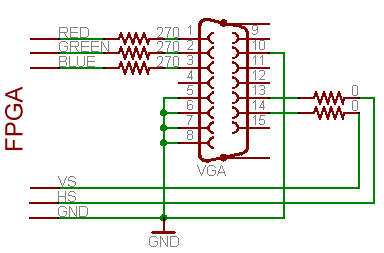
All in all the HW interface is quite simple as you can see in the picture below (from www.fpga4fun.com) .
The 270Ohm resitors are used to generate a voltage divider with the internal impedance of 75Ohm which, supplied with a 3.3V voltage, would give us roughly the needed 0.7V.
Ok, all this is cool, but how does it fit in the FPGA design?
Of course this would work nicely with an MCU or an FPGA, but I think the FPGA solution is more appropriate in this case since you can dedicate some internal circuitry to handle the synchronization signals and have it work in parallel with your solution.
One way to go is to design a vga_synch module that generates the HS and VS signals, plus calculates the current X & Y coordinates.
Then we will have another module to use such coordinates in order to calculate R,G and B based on a mathematical formula, conditions or reading values from RAM (like it happens in a PC VGA card).
Implementation of the sync module
For practical reasons (this is also the case in real world applications), one single clock will be used for both the HS and VS signals, so VS will have a period which is an integer multiple of the HS period.
Also, we will use the same base clock to calculate the width of those signals and every single pixel.
Instead of creating my own module I will present the one provided with my FPGA board, so credits goes to some unknown author.
I will however deeply comment every single part of it, comments are mine, therefore all the shame deriving from possible mistakes goes to me :)
Before discussing the module itself, I have to specify that the clk signal is obtained by multiplying by two (in a pll) the board 50MHz clock, so it is a 100MHz clock fed to the sync module.
I don't know why they decided for this frequency since they are then dividing it by 4 in the Verilog module and nowhere the 100MHz frequency seems to be used.
They could have just divided by two the 50MHz and skip the pll.. but maybe this module was used also for higher resolutions.
All this just defines an input clock (the 100MHz we discussed before) and reset, plus the 5 outputs being HS,VS, the X counter, the Y counter and a flag (Ready_Sig) which accounts for the front/back porch times.
This part is just used to implement the needed division by 4.
The variable Count1 is used and when it equals 3 (3'd3) it means 4 clock cycles passed (0 to 3), in other words a time lapse of 40ns (1/25MHz).
Conditions are : At reset restart from zero, at max count (T40NS) restart from zero, else just increment.
Now we calculate the X counter (at each clock)
The counter itself is defined as a 11bit number reg [10:0]Count_H; (which also makes us think this module might have been used for higher resolutions, since for the 640 one 10 bits would have been enough).
At reset, as usual, start all over from zero, if we reached column 800 -see, we calculate front porch and back porch as columns instead of times, it's easier this way!- then back to column zero else IF we are at the 25MHz marker (Count1 maxed) increase the X counter.
The Y counter mechanism is similar, with the only difference that it is reset to 0 when it reaches 525 and it is incremented when the X counter is maxed.
Now the isReady flag is calculated, it tells us if we are in the usable XY area or if we are in those black borders in which our R,G and B signals should be kept silent.
isReady is set true when X is between 144 and 784 (if you subtract them you obtain 640) and Y is between 35 and 515 (guess what you get if you subtract them? :) )
Finally VS and HS are calculated based on the X and Y counters, their duration is respectively 3 rows and 97 columns (you can convert these in times if you like).
Also note these signals are negative.
Finally the real coordinates are computed (if we are in the usable area, identified by isReady = true) by subtracting the left and top border.
Will close it here today, going to explain the control module in the next post, but that's the easy part.
I am back playing with FPGAs.
Meanwhile I bought a new FPGA borad, not that the tiny one I already had did not do, but I found that connecting and disconnecting stuff all the time to the GPIO was not really a convenient way to go.
So I went for another Cyclone IV board, a bit more expensive, but it has a bit of everything onboard.
Most of all it has external SDRAM, a VGA connector, Ethernet, an internal B/W LCD, some 7 segment leds, USB, a buzzer...
Looks like a perfect platform for Nios II stuff.
This board is a Black Gold Cyclone IV EPCE15 (15K LEs) which seems to be designed and built with some quality criteria in mind.
Not sure what the exact brand is as I found references to Alinx, heijin.org and OSH (you can see an OSH logo in the picture, top right).
The url on the bottom right part says http://oshcn.com , but that appears to be a domain for sale :)
Ok, not exactly a Terasic product, we get it, right?
Still they went the extra mile and packaged the whole thing in two plastic transparent sheets (laser cut), PCB finish seems to be really nice and you get an amazingly good looking box which even has magnets to keep the front flap closed (I know, it is a tiny useless detail, but at least it shows they are trying to give a quality image, which never hurts).
In my case the box contained the assembled board, a psu, an usb blaster with cables and a vga cable plus a container with 3 DVDs.
Yup, 3 DVDs of docs, samples, software, videos illustrating every single experiment included... which is all great provided you can read Chinese.
It seems there are detailed instructions for every single step, every single detail, but not a word in English.
Actually the parts datasheets are in English once you find them in a folder structure that has Chinese directory names.
Same thing if you try to find something in internet, looks like there is plenty of info there, but pretty much none in a language I can understand.
Looks like it's a good time to start learning Chinese, after all, I wish they taught me that instead of Latin back when I was young!
Now I already speak 3 languages (plus I can curse in Latin too, does that count as a 4th?) and about learning a 4th which has a complex and completely new (to me) alphabet... call me lazy, but, seriously, I am already trying to learn FPGAs, I might pass on this one!
Finally, scavenging in the discs and renaming folders in a way I can understand them, I found a lot of useful material.
Verilog is Verilog, schematics are schematics and to be fair there are very few times when I found comments that were decent enough to be somewhat useful, so, no big deal if they are written in Chinese after all!
Verilog modules and variables in the examples are in English, plus you get a separate folder with a full Quartus II project for each experiment.
I already tried most of the experiments and started to modify a few of them.
Particularly I focused on the VGA interface, which -at least on this board- is not really suitable for a practical purpose.
The signal appears not to be clean enough (might require some proper shielding) and the color depth is only 3 bit (1 bit per color component).
On top of that the voltage I get for each color component seems to be too low, so, what you would expect to be a white pixel (111) turns out to be a pale grey.
Maybe toying around with the IO bank settings on the Cyclone IV could solve that last issue.
That said, all is completely fine to run experiments and learning from them.
I will write another post about VGA, here a picture of a binary color pattern I did yesterday (is it a form of art? :) )
Meh, I know, kinda useless, right?
That's why I call it art!
Seriously that kind of experiment makes you realize how a VGA sync module works, how to interface with it etc and from a dev perspective, with FPGAs, the color depth does not change much your design.