While in theory it's all quite simple, the correct selection of components to be used is extremely important.
The basic Idea is that the MCU generates a pwm signal which controls the gate of the mosfet.
Practically a few things must be considered, in fact you might get away with it easily if you do not need a lot of current to go through your power mosfet.
If you have no idea on how mosfets work, you can check my post here.
It all comes down to the internal resistance between Drain and Source, you need it very high when the device is OFF and very low when the device is ON.
That's because if you are planning to have several Amps going through your transistor when it is on, you want a very low internal resistance or you will dissipate a considerable amount of heat (which is power you are wasting in whatever you are doing -except if you are doing a heating system-).
P = RI^2 from Ohm's law, so say you have 20 Amps and your R is 1 Ohm, you are dissipating 1*20*20 = 400W of power.
Mosfets tend to have a gate threshold (Vgs) at around 2 to 4V, however, while they "open" at that low voltage, their internal Rds resistance is still pretty high.
Every device has its own Rds curve in relation to the Vgs, but normally you want to drive the gate at about 12V or more.
You can find on the market some "logic level" mosfets that can be driven directly with a TTL signal, however they are normally not suitable to drive high currents and high voltages.
I chose a N channel mosfet for my experiment, particularly the IRF3710.
This device can deliver 46Amps at 100V with a reasonably low RdsON value (about 28mOhm) with Vgs over 7V.
Definitely it is not possible to drive it with a 3.3V signal.
A bit of math let's us find P = 46*46*0.028 = 60W which is still a lot, but I will probably be working in the range of 10Amps with way better results.
The problem with these devices is that to be able to let such big currents to pass through the channel, they need to create quite a big channel.
To open the N channel in the P doped semiconductor substrate, we will need a lot of charges, meaning the gate will act as a reasonably big capacitor.
We definitely need to charge that capacitor as quick as possible as a partial charge would result in a lower gate voltage which in turn would generate a higher Rds.
This means that not only we need to provide a sufficiently high voltage on the gate, but also we need to provide enough amount of current.
That's where gate drivers come in help.
They basically act as a "primary stage" mosfet to raise voltage and current to drive more efficiently the power device gate.
I was suggested to look into the Microchip TC4420 and similar devices.
This one particularly contains two logic level mosfets configured as a totem pole, that can output 18V and up to 6A.
These little buddies make your life way easier.
I first tested their output signal by feeding them the pwm signal of the MSP430G2 on one side and a 12V supply on the other.
(if you want to know how to output a pwm signal from the msp430g2, you can check here )
Despite the fact that I arranged the test on a solderless breadboard, I managed to obtain some decent frequencies.

As you can see in the picture I definitely have some (non desired) ringing, but that's probably reasonable if you consider all those jumper wires going around in the breadboard.
Normally with these circuits you need to keep very short traces on a nicely designed PCB, that would definitely help in reducing parasitic effects (inductance/capacitance etc).
Plus I did not add any filtering cap for now, which would also help.
The waveform in the picture is at 1.32MHz, not too bad after all on a breadboard.
The next step was to add the power mosfet, so I did setup a test circuit like this one :

The two channels of the Oscilloscope are used to plot the output of the gate driver and the output of the power mosfet.
A Load resistor is added to simulate some load on the line... and at my first attempt I was able to get the "magic smoke" out :)
The load was too high, not a problem for the mosfet because it can handle 46Amp and the PSU can only provide 20, it was not a problem for the PSU either... but the tiny jumper wire did not appreciate much the glorious 20A pulses.
Now they smell funny and they are bit "crusty", but they still work (with a higher R Load impedance).
Channel 1 of the scope measures Vds (voltage between Drain and Source) which goes to (almost) zero when the gate is fully open.
Technically it's the voltage across the internal Rds resistor, so if it goes nicely down to zero it means we successfully drive the gate.
I will need to repeat this test with a higher load on the line (but not on the breadboard, melted plastic does not smell really nice).

Channel 1 is red and the volt scale is 2V per division.
You can see the zero level being marked by the little (1) red marker on the left side.
Channel 2 is yellow, showing the gate driver output, the two signals are inverted since when the gate signal (yellow) is high, it closes the circuit, so the Vds (red) drops to zero.
That's what I get at 80Khz.
I increased the frequency at about 320KHz and the result is visible in the picture below.
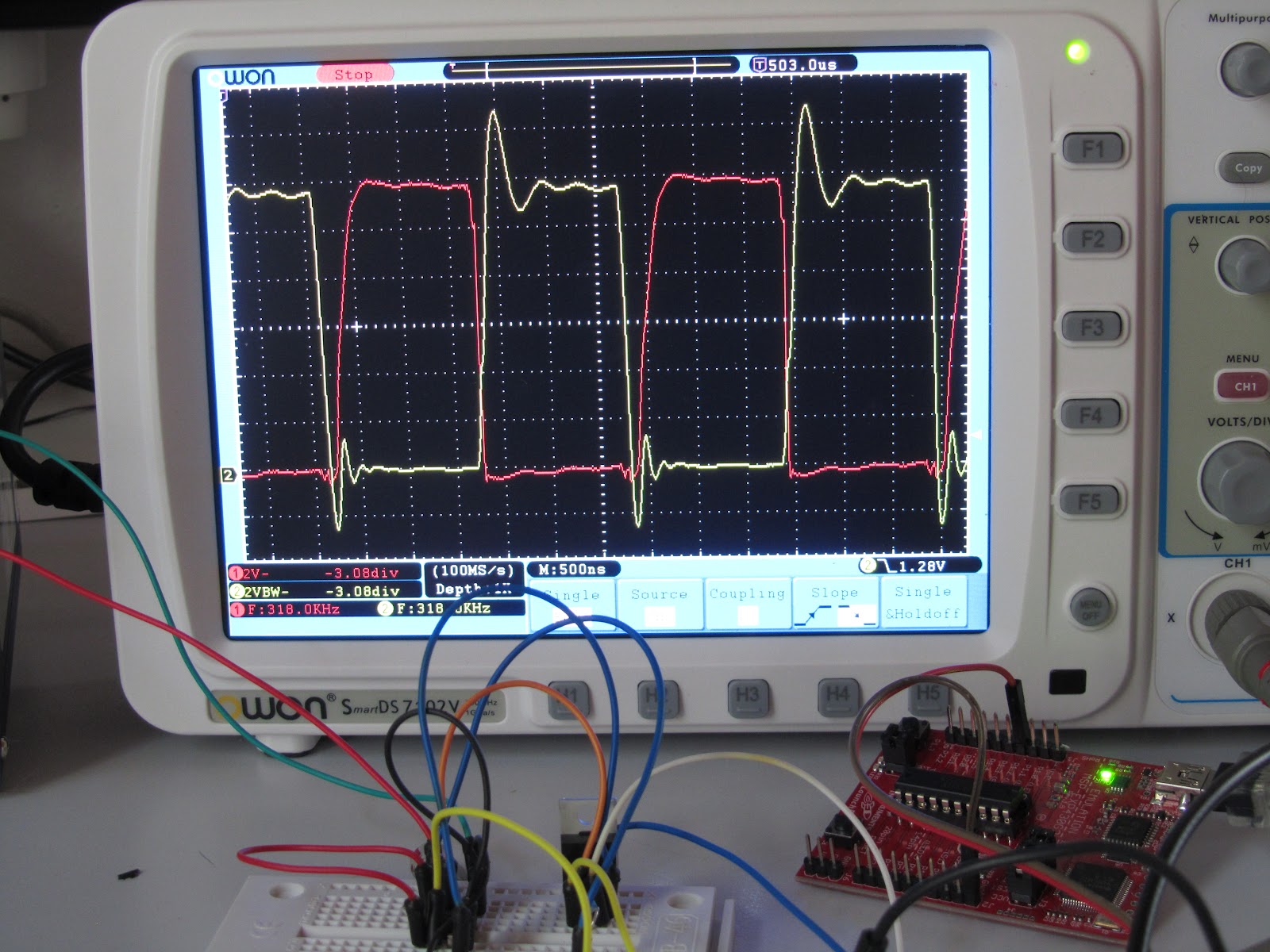
Both channels are now at 2V per division, aligned to their zero V.
You can see the rising edge of the Vds (red) being a bit "slow", that's definitely something that needs to be improved, which I assume can be achieved by discharging quicker the mosfet's gate.
Indeed proper cabling/pcb design is also needed, in fact the TC4420 can output up to 6A, no way that's going to happen using those tiny jumper wires.
I don't think it's something I can work on on a solderless breadboard like that, I probably need a better layout and definitely shorter connections.
Next step will be to add some caps, an inductive load on the output and a freewheeling diode, that's where the real "magic smoke" could happen :)
Update : adding a 10Ohm gate resistor on the mosfet the signal becomes like this :

Normally a fast diode should be placed in parallel with the resistor, to improve the shutdown of the gate (or at least this is what I understood reading this interesting document)
4 comments:
Hi Francesco,
Thanks for your help in my previous questions.
In fact, I am also trying to use the C2000 Launchpad to control my IGBT. I tried to read a lot, but still no idea on how to input my reference signal and how to get the output. I am asking if you can help write a couple of lines code to show me how to read my reference signal and how to get the output control signal.
For example, in your picture of the board. You have two wires connected to two pins. Can you advise me which one is the reference and which one is the control signal, and what code do I need to implement it.
Thank you very much
Sorry, I do not understand : what do you mean input and output the reference signal? which referece?
The two wires are : GND and PWM signal, but I was not driving directly the MOSFET as it was not a "logic level" mosfet, the one I used needs a higher voltage to open completely.
I used a driver as described which opens with the 3.3v signal coming from the launchpad PWM.
Then the driver gets as input voltage a 12V and modulates it with the pwm, outputting a pwm signal at 12V which finally works fine to open the gate of my mosfet.
Hi Francesco,
Thanks for your reply. Maybe my explanation was not very clear.
If I assume a buck converter is controlled to achieve a constant voltage at the output. Therefore, we have to give a reference voltage (say 20V). The actual voltage at the output should be measured to compare with the reference voltage. And then the IGBT can be controlled based on the difference. Hence, the reference voltage and measured voltage should be the inputs to the Launchpad. I am not sure how to do that.
Anyway, if that is different from what you have done here, do you mind to post your code here to give me some ideas?
Many Thanks
Hello again, my code is basically what you can find here.
I was not using any feedback and there is no "feedback input" functionality, instead you will need to use the ADC to monitor the the voltage venerated.
Indeed you will not be able to feed directly a 20V voltage to the ADC unless you want to toast it.
You will need to add a proper voltage divider.
Some kind of protection might also help, probably a zener diode BEFORE the divider (you should account for the voltage drop in the diode).
The idea is that your output from the divider will NEVER raise higher than 3.3V (or the reference voltage you use).
Alternatively you can also use the internal comparator (never tried personally), also for that one make sure your voltages are in the range accepted by the msp430.
Post a Comment